
Estimated reading time: 7 minutes
Hon Hai Precision Industry Co ltd is a name that may not be as commonly known as its more popular and trading version – Foxconn. Headquartered in Taiwan, Foxconn is also the largest private employer in People’s Republic of China (PRC or “mainland” China).
‘Traditionally’ Foxconn has been an “Electronic Manufacturing Services” (EMS) company – ‘manufacturing’ (or rather assembling) other company’s products like Apple’s iPhones, Microsoft’s Xbox and Sony’s Playstations – the chips (ICs) needed for them, one would assume, are supplied by established semiconductor fabs. When in mid-2019, Young Liu replaced the founder Terry Gou as Chair for the company, one of the news articles described Foxconn’s portfolio thus
Taiwan-based Hon Hai Precision Technology, which trades as Foxconn, focuses on the foundry service of electronics, research and development of precision electrical components, chassis, barebones, system assembly, optical communication components, liquid crystal display and other upstream and downstream products and services in the computer, communication and consumer electronics fields.
Prior to being promoted as Foxconn’s Chair Young Liu was the general manager of Foxconn’s semiconductor unit, in charge of the chip business and considered the semiconductor expert in Foxconn. Hence analysts have predicted that there will be an increasing foray by Foxconn into the semiconductor business . Add to it the fact that Young Lius position as head of the semiconductor division of Foxconn was perhaps replaced by Bob Chen (reference) who is ex-TSMC though seemingly with packaging experience
Earlier in 2016 Foxconn had acquired Japan-based Sharp in a $3.5 billion deal and Liu was made a company director. At that time, the move was seen by at least some western commentators as part of a “Chinese” expansionism in technology. An article in forbes for example said
That Sharp, one of the leaders and drivers in the technological innovation that underpins the global competitiveness of Japan’s consumer electronics industry, should fall into foreign hands, and especially Chinese hands (Hon Hai’s corporate base is in Taiwan, but its operating and–we guess–management ties with mainland China are so deep as to render it effectively a Chinese company), has for many at the top of Japan’s business and political establishment been unthinkable.
From a technology standpoint, the Sharp acquisition “was mainly interpreted in terms of Foxconn’s interest in Sharp’s OLED screen panels, especially as a main manufacturer for Apple’s iPhones” however Sharp also owned a 200mm (8 inch) semiconductor fab at Fukuyama which ran the 130nm(0.13μm) process node. The “Business Group S” said to be established in 2017 and headed by Liu prior to his taking over as Chair of the company, as per Foxconn website has been responsible for “semiconductor equipment, 8K TV SoC, panel driver IC, amplifiers and related operations”.
On 21 December 2018, Nikkei Asia reported that “Foxconn Technology is preparing to launch a $9 billion chip-making project in China as tensions intensify between Washington and Beijing over China’s tech ambitions”. The report further said that “Foxconn plans to build chipsets for ultra high-definition televisions and CMOS image sensors for phones in Zhuhai, with hopes to eventually expand into production of higher value chips for robotics and autonomous vehicles.Foxconn will also enter the foundry market, offering to build chips designed by other semiconductor companies. A majority of the cost of the fab will be subsidized by the city of Zhuhai”
In an analysis published a few days later and also quoting the Nikkei Asia news, EETImes opined that “Initially, Foxconn is expected to draw on Sharp, which has experience making CCD/CMOS sensors, LCD drivers, game console CPUs and other logic. [Sharp] has operated an 8-inch fab in Fukuyama at the 0.13μm process node. Foxconn’s 2016 takeover of Sharp provides the ability to design and produce semiconductors for the first time in Foxconn’s history as it shifts from electronics assembly to higher margin chip production… The aim is eventually to expand the 12-inch(300mm) chip facility in Zhuhai to make more advanced chips for robotics and autonomous vehicles”
200mm fabs typically run process nodes older than 90nm. Owning the technology know-how of running a 200mm fab with 130nm process node for chips with limited applications is far from being sufficient to be able to run a 300mm fab with say a 28nm technology. The analyst quoted in EETimes was of the opinion that “Over the long term, Foxconn may seek tie-ups with second- or lower-tier foundries as part of the chip fab plan” – note that there are only a handful of fabs that run 28nm in production
Not much details of the current status of the “Zhuhai fab” could be found in the public domain, in fact there seems to be very little updates available after that Dec 2018 news (or I may have missed). In reports like this that emerged in mid-2020 about Foxconn’s plans for new chip packaging facilities in Qingdao province there is a mention of “Over the past two years, Foxconn struck deals with China’s local governments in Zhuhai, Jinan and Nanjing regarding its participation in the local chipmaking sectors”. However information on the latest status of these are missing
In November 2020, there was news of Foxconn bidding for a stake in Silterra – a 200mm wafer fab owned by Khazanah Nasional Berhad, the investment holding arm of the Malaysia government. It offers CMOS manufacturing processes from 180nm down to 110nm with support for logic, analog and mixed signal, radio frequency, high voltage and MEMS applications. The bid however did not go through but by mid-2021 reports emerged that Foxconn may have obtained an indirect stake via “DNeX”
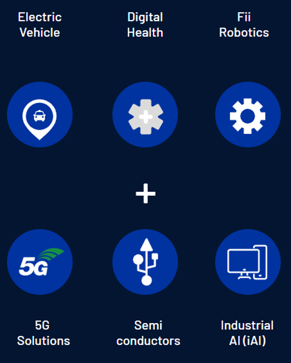
Meanwhile, Foxconn by now had officially announced its “3plus3” strategy – new industries focusing on electric vehicles, digital health, and robotics using artificial intelligence semiconductors and 5G technologies
Hence it was less surprising when in May 2021 Foxconn announced a joint venture named XSemi in collaboration with Taiwan based semiconductor component manufacturer Yageo or in August when there was news of Foxconn acquiring Macronix 150mm fab “targeting SiC semiconductors” and yet again in Nov there was news of it opening a design center in New Taipei
However, none of this can still explain where Foxconn can possibly get the technology for the 28nm fab that it has proposed in India along with Vedanta. Perhaps the ‘closest’ news of Foxconn getting a technology that is sub-100nm is this report from Sep 2021 which says “Hon Hai (Foxconn) would use TSMC’s 40-nanometer process to make battery management ECUs for the growing electric vehicle market”. It is however not clear which facility of Foxconn would be using this technology
Perhaps – and this is just a speculation – Foxconn is in talks with an established fab like TSMC or UMC for 28nm technology also, or it could be in talks with an Intermediate Research Organisation (IRO) like IMEC Belgium. In the case of an IRO however, what is obtained as technology is typically not a production ready one but a development stage one which may take 2-3 more years of further maturing to get to the yield levels required for high volume manufacturing. In such a scenario it is not clear whether Foxconn has a 300mm fab facility that it owns or has access to, where the technology could be made production ready by the time say a factory is built in India – perhaps the “Zhuhai fab” if indeed is close to being factory ready as a 300mm facility could be the answer, but there is not much information about it after the initial news in 2018
Meanwhile, on 14 March this year, WSJ reported that “Foxconn is in talks with Saudi Arabia about jointly building a $9 billion multipurpose facility that could make microchips, electric-vehicle components and other electronics like displays, according to people familiar with the matter” – so India may not be the only place where Foxconn is trying to newly venture into for semiconductors or related. This could also be part of its increasing efforts to “pivot away from China” as mentioned in this analysis
It looks like much of Foxconn’s plans and preparations in the semiconductor domain- especially on 300mm fabs- are either “still in the making” or are intentionally kept under the wraps. With such a lack of availability of easily accessible and clear information this attempted compilation by me is also likely an incomplete one.
Also Read:
- Why Shaurya Aeronautics’ Removal From US Sanctions List Matters Most to India’s MRO Industry?
- The Mirage Of Aircraft Brokerage: Why 90% Aspiring Aircraft Brokers Never Close a Meaningful Deal

- AI Can Now Diagnose 102 Brain Tumour Subtypes in Minutes. But Who Gets Access?

- Aircraft That Predict Own Failures – Reason Why Aircraft Health Monitoring Market is Racing To $8.6 Billion

- The Indian Army Officer Recruitment System: Leadership, Selection and the Future of Military Command

- Kerala: Leveraging The Past, A New Era Of Hope & Progress Begins


