
Estimated reading time: 6 minutes
On 15 Dec 2020, the government through its Ministry for Electronics and Information Technology (MEITY) issued an Expression of Interest (EoI) for setting up semiconductor fabs in India. Companies that the government hopes to get in India through such a move, fabricate semiconductor chips (ICs), essential for electronic gadgets.
On 16 March 2021, a similar EoI was issued for display fabs which make display units for gadgets
Both EoIs were closed for applicants on 30 April 2021 and on 21st May, The Financial Express quoted Ajay Sawhney, Secretary to MEITY, as saying: “We are working to formalize an incentive structure for setting up display as well as semiconductor fabs in the country. In the coming six months, we will try to come out with a concrete proposal”.
Who all submitted their proposals on the EoIs before the deadline has not officially been disclosed by the government yet. Unofficially and indirectly, through an Independent Association, a report was put out in June 2020 “Over 20 semiconductor manufacturing and designing companies in high-end, display and specialty fabrication have submitted expressions of interest (EOIs) to set up manufacturing plants in India. Of this, two-three are ‘very serious’ projects, according to the India Electronics and Semiconductor Association (IESA)”
This author was able to bring out to the world details of one of the proposals in an interview with Ajay Jalan, founder and MD of ‘Next Orbit Venture Funds’ published in Swarajyamag on 31 July 2021 – “We want to build a world-class semiconductor manufacturing fab with a target market of analog and mixed-signal, wafer size 300 mm (12”) with fab capacity of 40,000 wafers stats per month in two phases. The technology node for this Analog Fab is 65 nm, where products are logic, mixed-signal, CMOS Image Sensor, power management, RF CMOS and RF SOI”
Just in case any of the readers are wondering “Why 65nm ?” when the state of the art in overall chip manufacturing is 5nm and a roadmap is there for 3nm in 2022, 2.1nm by 2025, 1.5nm by 2028, 1nm by 2031 and 0.7nm by 2034 and so on, you may want to read this article and also more about Analog fabs and the technologies used or planned to be used in the kind of products mentioned in the above quote. Also, India needs to stand up first before it tries to walk and run, and to stand up on its feet, demonstrate its capability and to trigger more later, a 65nm commercial Analog fab will be a good choice
Ajay Jalan in his interview had also mentioned that his group has a “Letter of Intent with one of the top 5 foundries for digital fab”. Though in the interview, Ajay did not mention which fab, in the picture given, Taiwan based United Microelectronics Corporation (UMC) was mentioned as part of the bigger plan.
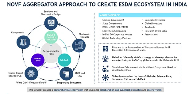
Ajay had also mentioned- Our tech partner, among the top three in the world, has assured us that once we create semi infra and a supply chain through analog fab, they will come for 28 nm digital or lower node as per Indian market requirement at that point of time.
Media reports on India and Taiwan being in talks has been there throughout the year and from September onwards, speculations were also about a possible $7.5 billion cost digital fab in the plan. In September itself, financial express also reported “The government is aiming to lay the foundation of the country’s first semiconductor manufacturing unit by June-July next year and a request for proposal (RFP) will soon be floated seeking commercial bids from companies” . The report also had quotes from MEITY minister Ashwini Vaishnaw.
On 15 Dec 2021, on the first anniversary of the govt floating the EoI for semiconductor fabs, government of India formally approved $10b for development or semiconductor and display manufacturing ecosystem in India – a press release with summary of the policy can be found here and a “101” article on the significance of the move can be read here.
Interestingly, the very next day, Hindustan Times reported about “India and Taiwan in talks” with “Both sides are eyeing the possibility of one of Taiwan’s semiconductor giants, including Taiwan Semiconductor Manufacturing Company (TSMC) and United Microelectronics Corporation (UMC), setting up a facility in India. The Indian side has proposed several sites for the hub though the two sides are yet to come to a final decision”. If that were to be believed, there is no breakthrough yet and we will have to wait further to know whether it is a Yes, No or “later” from TSMC
There are also rumors coming in from some quarters that the talks may be in a “soon to be agreed upon and made public” stage – less likely that it will be government of India who will confirm or deny this as it is meant only to be a facilitator possibly for a direct investment by those MNC fabs or a deal between the MNC and an Indian business group.
A TSMC or UMC, if indeed interested, is likely to go for a 20 or 22 or 28nm digital (logic) fab, possibly along the financial model of what is coming up in Japan. If that happens, it can be complementary to the Analog fab, however, the question arises as to how long should India “wait” for a ‘deal’ to be finalized.
NOVF has welcomed the 15th December announcement and thanked Government of India for agreeing to 50% incentives, but also added the following as per a report in economic times on 16th December. Quoted paras below:
The concerns are slightly different for players like Abu Dhabi-based Next Orbit Ventures, which formed a consortium with Israeli Tower Semiconductor and floated an Expression of Interest (EoI) for a $3 billion analogue 65-nanometre semiconductor fabrication unit in Dholera, an industrial hub in Gujarat.

"The only thing we want to make sure of is that the approval should be given to EOI applicants soon. We have been ready for ground-breaking since the last one year," Ajay Jalan, founder and managing partner of Next Orbit Ventures told ET. It should not happen that the approval of the incentive will take another year's time because we submitted the detailed project plan to the government in response to the EOI." Read more here:
Do we have a timeline from the government ? In an interview published in Economic Times right after the announcement of the scheme, Minister Ashwini Vaishnaw was asked “how soon can some of the large units get approvals?” and he replied “Very fast, very soon, a few months … You can expect good action in the coming four-six months’ time frame”
In other words, he is perhaps still hopeful of ground breaking happening in June or July 2022 – whether it is of Tower semiconductor supported “ISMC” (as Ajay Jalan seems indicated how they would name) or also a TSMC or UMC, will hopefully be clearer in the upcoming months.
It may be prudent for government of India to “help the bird in hand” at the earliest, while it can continue to woo the “two birds in the bushes”. Ground breaking of a Tower semiconductor backed ISMC may be the much needed inflection point India has waited 2-3 decades for.
Also Read:
- AI Can Now Diagnose 102 Brain Tumour Subtypes in Minutes. But Who Gets Access?

- Aircraft That Predict Own Failures – Reason Why Aircraft Health Monitoring Market is Racing To $8.6 Billion

- Google Ads Optimization Techniques for 2026

- India’s Aircraft Engineers Are Revolting – And Aviation Can No Longer Ignore Their Anger

- With Keyboard Era Quietly Ending – India Set To Benefit The Most

- NeoCloud Engines: The Hustlers of AI Compute


