
In case you wondered if the fourth word of the title of this article has a spelling mistake, the answer is a ‘No’. The title is an intentional combination of Pepsi’s popular advertising slogan from the 90s – Yeh Dil Maange More (literal translation: This heart asks for more) – with the last name of Gordon Moore who in 1965 as Director of the Research and Development lab at Fairchild semiconductors made some observations and 10-year predictions in a report, which later got extrapolated and ‘adjusted’ as the now famous “Moore’s Law” and the first name of Morris Chang whose mention will happen a bit later in the story.
For the uninitiated, transistors form the fundamental building blocks of most Integrated Chips (ICs). Moore’s Law – with the extrapolations and adjustments – predicts that the number of transistors in the ICs double almost every two years. A few years after that report, along with Robert Noyce (inventor of the monolithic IC), Gordon Moore founded the NM electronics, named after the first letters of their respective last names. NM electronics was soon renamed as Intel, a name that comes first to most people’s mind when they think about electronics in general and IC manufacturing semiconductor fabs (or foundries) in particular. However, those who are a bit more familiar with the field know that the story of fabs will be grossly incomplete with the mention of just Moore or Intel.
Robert Dennard, credited also for the invention of the transistor-capacitor based memory cell (which formed the basis for the Dynamic Random Access Memories or the DRAMs), in a 1974 paper set the base for what would be later known as Dennard scaling, guiding much of what happened later in shrinking sizes of transistors. In fact it is Dennard who is credited with predicting or setting the standard for the 0.7 ratio (square root of 0.5) for channel length between generations of transistors – which would mathematically mean halving the area (due to similar scaling down of other dimensions of the transistor as well), increased speed or operating frequency (because the carriers now has lesser distance to travel), reduced voltage needed (as the electric field needed is inversely proportional to the distance) and hence reduced power .
I could be wrong, but reading through their original papers, I do not see Moore explicitly talking about ratios for transistor scaling nor Dennard mention how many years it would take between generations of scaling – perhaps it is the combination of their observations that led to the expectation of transistor scaling and new generations every two years. Dennard was appointed an IBM fellow and IBM more or less diligently followed the size ratio, for example its 1994 “CMOS-5X” was based on 350nm technology and was followed predominantly by 180nm, 130nm, 90nm, 65nm, 45nm, 32nm and 22nm (year 2013), by which time it decided to sell its production fabs.One can see that it is 7 or 8 generations (or nodes) in a span of about 19 years, so though may not be exactly 2 years, the scaling happened and continues to happen.
Both IBM (up to 2015) and Intel continued to be what can be called Integrated Device Manufacturers (IDM), a model in which they sell products that use the ICs manufactured at its own fabs, but also whereby the fabs can in theory be also used to manufacture ICs designed by fabless companies as long as the platforms and technology matched. In fact not just fabless companies, but even other IDMs would sometimes get their IC designs manufactured at fabs owned by other IDMs, and one such example was Texas Instruments (TI) getting some of its chips manufactured in IBM fabs. One of them who would be involved from the TI side – Morris Chang – a Chinese born, would go to Taiwan a few years later and introduce a new business model by separating the manufacturing part (or the “make” part) from the “design” and the “create” part. Taiwan Semiconductor Manufacturing Company (TSMC) founded by him in 1987 was the first “pure-play foundry” and now the world’s biggest with over 50% market share among foundries
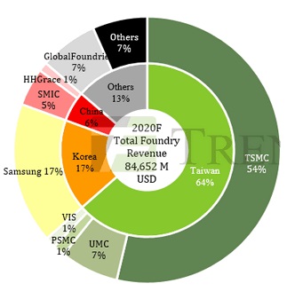
Talking about market shares and industry leaders is a bit tricky when it comes to semiconductor companies because one could see different sets of leaders and numbers depending on what you are looking at. For example, when it is said that TSMC leads the foundry market with over 50% market share, it is among those who report their foundry revenue – that is, all pure-play foundries as well as IDMs like Samsung. Below is one such chart, though numbers may not be perfect as it is from Dec 2020. Out of a total revenue of about $85B for the year, TSMC leads with about $45B and Samsung is second with about $14B .
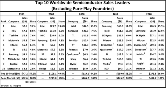
Here is a chart of what is being called “Semiconductor Sales Leaders”, but excluding the pure-play foundries and which is taken from an article detailing about the Intel-Samsung competition over the last decade for the top spot
Is there a “combined” chart ? I could find the following chart, note that OSD stands for optoelectronics, sensor and discrete components. The revenue of the companies which do not own a fab as well as the non-foundry revenue part of the IDMs can be considered the “chip or product sales” revenue
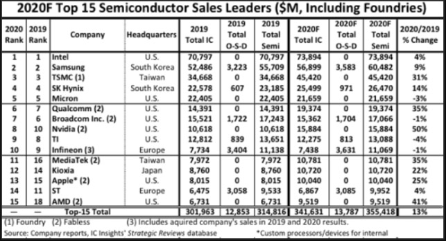
The numbers are slightly different in various charts, however together they give a good idea of the big picture. Though I could not separately confirm, it appears that the $60B+ revenue for Samsung includes the foundry service revenue of $14B+ . Intel though an IDM, over the past decade or even earlier had not offered its foundry services much for other companies and so would have relatively negligible foundry services revenue. However, its new IDM 2.0 strategy announced on 23 March 2021 says “Intel is establishing a new standalone business unit, Intel Foundry Services (IFS)” an indication that it wants to capture some of the foundry services revenue as well going forward.
In the continued race for transistor scaling and to claim to be the first to realise the next generation four big companies – Intel, IBM, TSMC and Samsung – play a role in their own ways. Note that standards of what can be called the next-generation node at some point started differing based on the type of platforms used as well the companies that drove them and so something like 65nm-45nm-32nm-22nm is not the only scaling path, 60nm, 40nm, 28nm, 20nm etc exist too. One can look at them as multiple paths or “half-nodes” in between one path of nodes, whichever way, the next significant set of nodes that race is on for are the sub-10nm ones – 7nm, 5nm, 3nm and now the 2nm
Let us briefly examine the current status of each of those companies. Over the past decade or so, Intel lost some ground as one of topmost fabs, its 10nm program was delayed and has been struggling with its 7nm in-house process. Reports say that Intel’s first 7nm chips will arrive in 2023 and that too using TSMC technology with further indications that the collaboration may go on for TSMC 3nm technology as well – in line with the section “Expanded use of third-party foundry capacity” of its IDM 2.0 strategy. Intel’s lagging behind has prompted some like the author of this article to write ‘two-and-a-half leading-edge fab makers’ – Intel counted as half (currently down but with a possibility to bounce back) and TSMC and Samsung the others . At least by the last quarter of 2020, there were commercial chips using TSMC’s 5nm process in the market. As per this Apr 2021 report, TSMC is expected to have a 4nm variant as well as its 3nm process in production in 2022, 2nm is currently in development and beyond-2nm in R & D. Note that TSMC is expected to continue to use “FINFET” technology (details of which are beyond the scope of this article) even at the 3nm node.
Also Read:
Even though IBM sold its production fabs, it continues to run a research fab at Albany where early development of advanced node processes are achieved and patented. In June 2017 it announced its 5nm process based on GAAFET (again, beyond the scope here) as opposed to FINFET. Samsung collaborated with IBM and by July 2020, there were reports of it being in production. Some reports suggest that Samsung did “risk production” of 5nm chips by 2018 itself while TSMC did it only by 2019 and that even in final production it may have been slightly ahead of TSMC. However things can get a bit complicated in such claims because timelines and complexity for different kinds of chips – for example memory chips vs processor chips for mobiles or tabs vs CPUs or GPUs for laptops could all vary. Moreover, foundries are often bound by rules from its clients (like Apple) in terms of how much they can reveal. Meanwhile Samsung also customized the GAAFET technology and came up with the MBCFET technology – both are nanosheet based – which it is planning to use for its 3nm offering and is expected to be in production by 2022,
IBM research ‘moved on’ and on 6th May 2021 announced successful development of the 2nm process and as this author quotes in his article , “they’re working, all we need is a fab”. Interestingly on 25 March 2021, there was an announcement that “IBM and Intel announced an important research collaboration to advance next-generation logic and packaging technologies”. Does that mean Intel may buy the 2nm technology (the early stage development) and take it further to production by sometime like 2024 and make up some, if not all of the lost ground in its competition with TSMC and Samsung ? Would the US govt be involved in some ways as after all both Intel and IBM are “US companies”. Or will it be yet again Samsung that would take IBM’s innovation to production ? Will TSMC “finally” break away from its FINFET based offerings and embrace GAAFET based ones ? These are questions that many semiconductor enthusiasts will be eagerly looking forward to for an answer.
Till now, I have not even touched upon two related subtopics – one, China’s growing ambitions in the foundry business as well its effort to reduce electronic imports and two, the chip shortages leading to stoppage of automobile production lines among other things. Both are topics about which plenty of articles have already been written in the media, including many in India based ones. In fact on the second subtopic, for the past 2-3 months almost every other day I stumble upon a new article, many quoting various CEOs on how long they think the chip scarcity may last and the years vary from end of 2021 to 2022 to 2023 and some even beyond.
While I do not want to go into those details, suffice to say that the field of semiconductor chip manufacturing has also become much more geopolitically significant recently. Multiple governments are known to be either offering or planning to offer sops to the giants, and yet again almost every other week, there is something new being put out on this topic – for example, within the last 7-8 days itself, there were reports of the possibility of TSMC going cold on EU request and probably investing more in the US including in 3nm plant, reports of US Senate including $52B to “bolster domestic semiconductor manufacturing”, while South Korea announced spending $450B over the next 9 years to take the lead in the global semiconductor market and Samsung on its part, raised its previously announced plans of spending nearly $120B till year 2030 to about $150B
Having come this far, how can I stop without writing at least something about India related to this topic ? My first media article on the topic of semiconductors, or to be more specific, on the need for commercial semiconductor #FabInIndia was published by News4masses on 21st May 2020 – exactly one year back. This article is in one sense my “anniversary article“, an expression of gratitude to N4M as in that one year I was fortunate to publish 17 articles in 3 media and also contribute in other ways including TV Panel discussions and videos, links to all of which are usually compiled and kept as a pinned tweet on my twitter profile
It is also in another sense a sad realisation that while key players and governments in other countries are moving at a much faster pace in making decisions as well as putting those to action, in India we are still at the mercy of multiple challenges – among other things an already slow decision making process, if anything made worse due to Covid and especially the second wave impact. The only real ‘development’ to report after my 8-April-2021 article in Swarajyamag is that the deadline for proposals for fabs based on an Expression of Interest (EoI) put out by the government on 15-Dec-2020, was not extended further beyond 30-Apr-2021.
Last heard is that the ministry is still evaluating the proposals it received and based on inputs or demands from them, will formulate a scheme to incentivise fabs in India. I continue to stress upon two points – one, that India need not right away shoot for fabs running the latest technology node and two, India need not wait for the biggest player. Start funding the good proposals that it received before it becomes too late for even them to be of relevance. Once it is proved that the infrastructure and ecosystem can be established in India, with proper planning ahead, within the next decade or so, in all likelihood bigger players and advanced technologies can be attracted. Very often, getting something started is the tough part – and I hope that the government of India will not let down any good proposal that has offered to do so, even if not the perfect one the government hoped for. After all, for the heart to desire more, there should be something to begin with.


